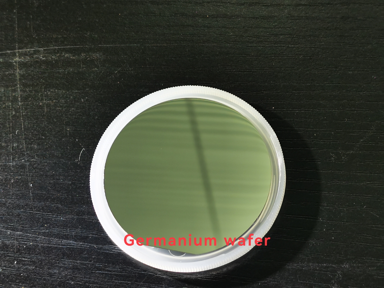
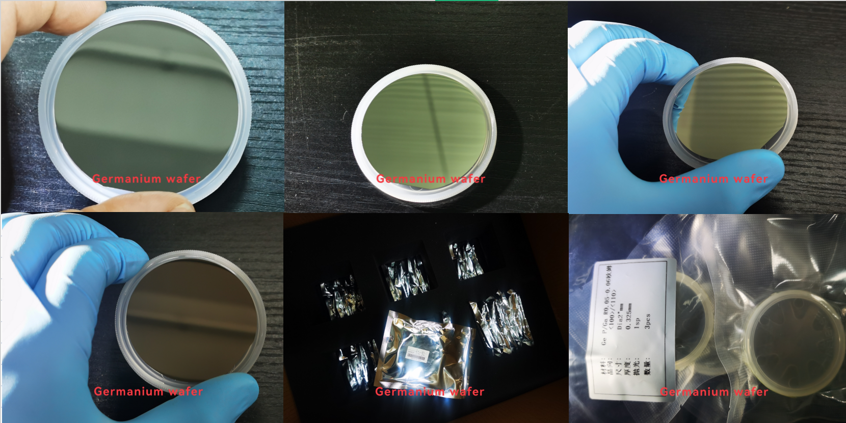
2inch N-type single side polished Ge wafers Germanium substrate Ge window for infrared Co2 lasers
Diameter:25.4mm Thickness:0.325mm
Shanghai Famous Trade Co,.Ltd offers 2”, 3”, 4”, and 6” germanium wafers, which is short for Ge wafers grown by VGF / LEC. Lightly doped P and N-type Germanium wafers can be also used for the Hall effect experiments. At room temperature, crystalline germanium is brittle and has little plasticity. Germanium has semiconductor properties. High-purity germanium is doped with trivalent elements (such as indium, gallium, and boron) to obtain P-type germanium semiconductors; and pentavalent elements (such as antimony, arsenic, and phosphorus) are doped to obtain N-type germanium semiconductors. Germanium has good semiconductor properties, such as high electron mobility and high hole mobility.
Germanium Wafer Process
With the advancement of science and technology, the processing technique of germanium wafer manufacturers is more and more mature. In the production of germanium wafers, germanium dioxide from the residue processing is further purified in chlorination and hydrolysis steps.
1) High-purity germanium is obtained during zone refining.
2)A germanium crystal is produced via the Czochralski process.
3)The germanium wafer is manufactured via several cutting, grinding, and etching steps.
4)The wafers are cleaned and inspected. During this process, the wafers are single-side polished or double-side polished according to custom requirements, epi-ready wafer comes.
5)The thin germanium wafers are packed in single wafer containers, under a nitrogen atmosphere.
Application of Germanium:
Germanium blank or window are used in night vision and thermographic imaging solutions for commercial security, fire fighting and industrial monitoring equipment. Also, they are used as filters for analytical and measuring equipment, windows for remote temperature measurement, and mirrors for lasers.
Thin Germanium substrates are used in III-V triple-junction solar cells and for power Concentrated PV (CPV) systems and as an optical filter substrate for a long pass SWIR filter application.
General Properties of Germanium Wafer
| General Properties Structure | Cubic, a = 5.6754 Å |
| Density: 5.765 g/cm3 |
| Melting Point: 937.4 oC |
| Thermal Conductivity: 640 |
| Crystal Growth Technology | Czochralski |
| Doping available | Undoped | Sb Doping | Doping In or Ga |
| Conductive Type | / | N | P |
| Resistivity, ohm.cm | >35 | < 0.05 | 0.05 – 0.1 |
| EPD | < 5×10³/cm2 | < 5×10³/cm2 | < 5×10³/cm2 |
| < 5×10²/cm2 | < 5×10²/cm2 | < 5×10²/cm2 |
Product detail:
mpurity level less than 10³ atoms/cm³
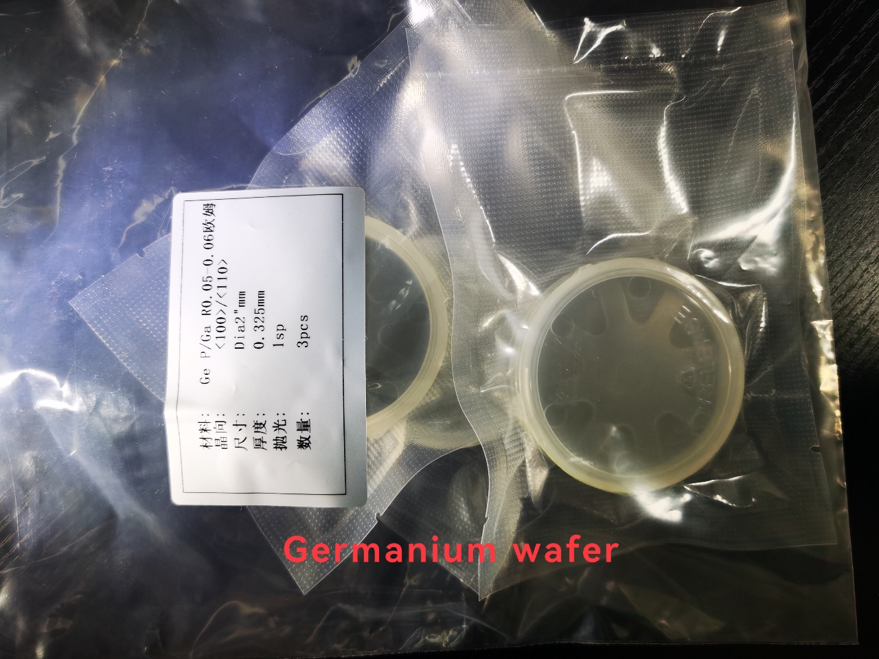
Material : Ge
Growth : cz
Grade : Prime grade
Type/dopant : Type-N, undoped
Orientation : [100] ±0,3º
Diameter : 25.4 mm ±0,2 mm
Thickness : 325 µm ±15 µm
Flat : 32 mm ±2 mm @ [110]±1º
Resistivity : 55-65 Ohm.cm
EPD : < 5000
Front side : Polished (epi-ready, Ra <0,5 nm)
Back side : Ground/etched
TTV : <10; BOW :<10; WARP :<15um;
Particles : 0.3
Laser marking : none
Packaging : single wafer
Q1. Are you a factory?
A1:Yes, we are a professional manufacturer of optical components, we have more than 20 years experience in optical cold working.
Q2. What is the MOQ of your products?
A2:No MOQ for customer if our product is in stock, or 1-10pcs.
Q3:Can I custom the products based on my requirement?
A3:Yes, we can custom the material, specifications and optical coating for your optical components as your requirement.
Q4. How many days will samples be finished? How about mass products?
A4: Generally, we need 1~2 days to finish the sample production. As for the mass products, it depends on your order quantity.
Q5. What's the delivery time?
A5: (1) For inventory: the delivery time is 1-3 working days. (2) For customized products: the delivery time is 7 to 25 working days. According to the quantity.
Product Tags:

|
|
SSP Germanium Semiconductor Substrate Ge Wafers For Infrared Band 100 / 110 2 Inch Images
|