2inch 4iinch 6Inch Sapphire based AlN templates AlN film on sapphire substrate
2inch on sapphire substrate AlN Template layer Wafer For 5G BAW Devices
Applications of AlN template
Our OEM has developed a serials of proprietary technologies and the-state-of-the art PVT growth reactors and facilities to
fabricate different sizes of high-quality single crystalline AlN wafers, AlN temlpates. We are one of the few world-leading
high-tech companies who own full AlN fabrication capa�bilities to produce high-quality AlN boules and wafers, and provide
profes�sional services and turn-key solutions to our customers,arranged from the growth reactor and hotzone design,
modeling and simulation, process design and optimization, crystal growth,
wafering and material characteriza�tion. Up to April 2019, they have applied more than 27 patents (including PCT).
Specification
Ch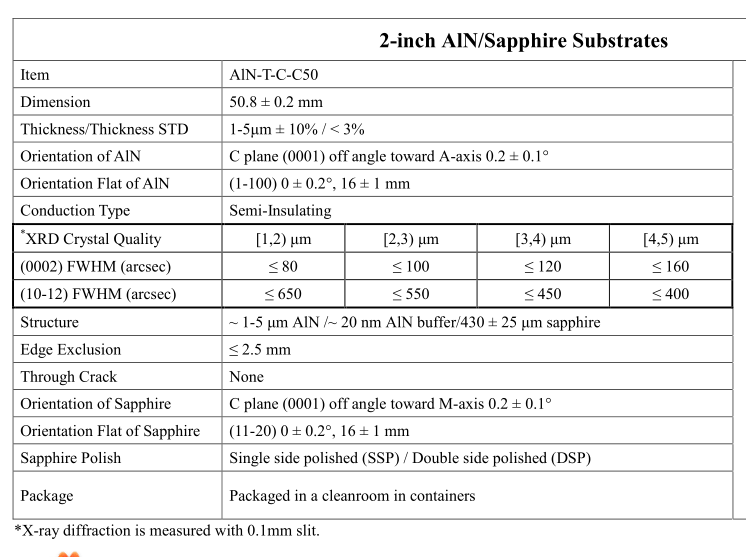 aracteristic Specification
Other relaterd 4INCH GaN Template Specification
| | GaN/ Al₂O₃ Substrates (4") 4inch |
| Item | Un-doped | N-type | High-doped N-type |
| Size (mm) | Φ100.0±0.5 (4") |
| Substrate Structure | GaN on Sapphire(0001) |
| SurfaceFinished | (Standard: SSP Option: DSP) |
| Thickness (μm) | 4.5±0.5; 20±2;Customized |
| Conduction Type | Un-doped | N-type | High-doped N-type |
| Resistivity (Ω·cm)(300K) | ≤0.5 | ≤0.05 | ≤0.01 |
GaN Thickness Uniformity
| ≤±10% (4") |
Dislocation Density (cm-2)
| ≤5×10⁸ |
| Useable Surface Area | >90% |
| Package | Packaged in a class 100 clean room environment. |

| Crystal structure | Wurtzite |
| Lattice constant (Å) | a=3.112, c=4.982 |
| Conduction band type | Direct bandgap |
| Density (g/cm3) | 3.23 |
| Surface microhardness (Knoop test) | 800 |
| Melting point (℃) | 2750 (10-100 bar in N2) |
| Thermal conductivity (W/m·K) | 320 |
| Band gap energy (eV) | 6.28 |
| Electron mobility (V·s/cm2) | 1100 |
| Electric breakdown field (MV/cm) | 11.7 |
Product Tags:

|
|
2 Inch Sapphire Substrate AlN Template Layer Wafer For 5G BAW Devices Images
|